
 SHIPS TODAY
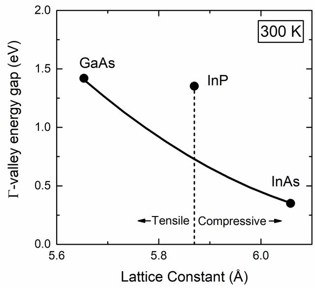
Introduction
In the past RPMC has taken a look at laser diode lifetime in both a white paper titled “How to Improve Laser Diode Lifetime! Advice and Precautions on Mounting,” and an application note called “Understanding Laser Diode Lifetime.” Additionally, we have explored the fundamental material structure of laser diode bars in a blog post titled “Understanding Laser Diode Arrays,” back in September of last year.
In this application note, we plan to combine these two topics and look at one of the key factors that affects laser diode bar lifetime – stress and strains. Despite the extreme power output of laser diode bars and stacks, which can exceed 2 kilowatts of power in quasi continuous wave (QCW) operation, the facet coating technology has improved to the point where it can handle intensities well over 20MW/cm2 making catastrophic optical damage (COD) no longer a limiting factor. With modern day diode bars, thermal management, mechanical stress, and material defects introduced by the mounting/packaging process are far more critical to their lifetime and performance. For this reason, we are going to focus our attention on both intrinsic and extrinsic stress in the diode, and how each affects the performance and lifetime of the diode.
Intrinsic Factors
To understand the intrinsic stresses and strains within a laser diode bar, it is essential to first take a step back and understand the importance of lattice matching between the diode and its substrate. It is relatively common knowledge among laser engineers that the stoichiometry of the diode material (the relationship between the relative quantities of the base elements making up the material structure) determines its bandgap energy and therefore it’s center wavelength. But as the stoichiometry varies so too does its lattice constant. While small, this change does lead to a slight lattice mismatch which adds either compressive or tensile strain to the active area of the diode, as shown in the figure below.

While this may appear to be problematic, diode fabricators are actually able to use the strain to their advantage. This is because it turns out that compressive strain slightly increases the bandgap and tensile strain decreases it, allowing for additional fine-tuning of the center wavelength above and beyond the stoichiometry itself. Additionally, it can be shown that when the active area of the diode experiences tensile strain, the emitted laser light is TE-polarized, and when it is under compressive strain, the polarization flips and becomes TM-polarized. The exact physics beyond these processes is far beyond the scope of this application note, but it is beneficial to have a basic understanding of these principles. For example, if a variation in the polarization or center wavelength is detected after mounting a diode bar, then it is an explicit sign of the process induced extrinsic strain.
Extrinsic Factors
The simplest way to explain extrinsic strain is that it is any process induced strain experienced by the diode bar. This could be created by point defects in the laser structure itself due to poor fabrication techniques, induced during the metallization process, or by the solder and heat sink. Since the fabrication and metallization steps are generally out of your control, for the remainder of this application note we are going to focus our attention on the soldering and heatsinking. That being said if all other factors are equal and you see a large lot to lot variations in polarization and center wavelength that could be indicative of fabrication and metallization issues.
As we discussed in our previous application note, when packaging a diode laser, choosing the appropriate solder preform for the die-bonding process is the critical first step for ensuring long term reliability, since the solder joint serves as the primary thermal conductor for heat dissipation. As a result, soft solders such as In are generally preferred because the flexibly of the solder helps to mitigate the stress caused by the mismatch of coefficient of thermal expansion (CTE) between the chip and the submount. An additional benefit of utilizing In solder is the relatively low melting point (157oC), which reduces the thermal load on the diode during the bonding process while soft solder can suffer from greater thermal-fatigue and creep-rupture than hard solders such as AuSn, the risk of cracks in the die or detachment of the die during thermal cycling because of CTE mismatch often outweigh any advantages of AuSn.
In addition to the catastrophic risks discussed in the previous application note, if the soldering step is not properly performed, it can result in an uneven joint thickness resulting in both static and dynamic stresses as the diode bar is temperature cycled. While this is most certainly an issue in all diode soldering the sear size of a laser diode bar, leads to an increased risk of a stress gradient forming across the length of the bar. For example, based on the difference in CTE between a 10mm GaAs diode bar and a copper heat sink, the difference in expanse can be greater than 10 microns. If this is exacerbated by uneven solder flow, overtime this repeated fluctuation in stress across the diode can lead to mechanical degradation and eventually failure. In addition to uneven flow, insufficient thermo-mechanical contact between the diode bar and the heat sink will also cause thermally induced stress gradients. Therefore, it is often useful to employ a methodology to prevent oxidation of the indium solder, removing the need for a reduction step, which often leads to solder voids.
The most critical factor when producing high output powers is the increase in temperature experienced during operation. New actively cooled expansion-matched heat sinks have been developed, to reduce the high thermal resistance in expansion matched packages with submounts. Typically, submount materials have a lower thermal conductivity than copper, which decreases the thermal load of the laser bar. Some examples are of common submount materials are aluminum nitride, beryllium oxide, and CVD diamond which all have a lower CTE than copper, but the material which tends to have the least degree of CTE mismatch for GaAs laser diodes is copper tungsten. In addition to being a good match for the diode bar itself, copper tungsten is also reasonably well matched with glass; this makes it easier for mounting optical elements such as cylindrical lenses directly to the package.
For extremely high-power applications it is typical for diode bars can be stacked and put into a single package capable of producing kilowatts of laser power. In this case, there is so much heat that needs to be removed from the stack that, microchannel cooling is often used to a large amount of waste heat in a small area. As a general rule of thumb, whenever a component’s heat dissipation levels exceeded roughly 500 W/cm2, conventional air-cooling systems are inadequate for removing excess heat. Forcing a fluid through a large number of small channels increases the level of heat transfer from the diode bar into the flowing liquid and allowing for laser diodes to produce the kilowatt levels of power described earlier without succumbing to terminal levels of thermo-mechanical stress.
Final Thoughts
Now that you have an understanding of the effects of stresses and strains on the performance and lifetime of laser diode bars, it should now enable to you better understand why specific packaging methods are preferred over others. Additionally, by understanding the relationships between polarization and bandgap energy and intrinsic strain, you should now be able to diagnose external strain based on how these outputs vary after packaging. Here at RPMC lasers, we offer a wide variety of high-power laser diode bars from Jenoptik in Germany. These bars are available as individual unmounted and mounted laser diode bars, packaged bars and stacks, and fully integrated fiber coupled modules. Depending on the output power and package cooling these lasers can either be run in continuous wave (CW) or quasi-continuous wave (QCW) operation.
For detailed technical specifications on our laser diode bars and stacks click here or talk to one of our laser experts today by calling 1-636-272-7227.
Be sure to check back for regular updates to our new application notes page.
Here at RPMC lasers, we offer a wide variety of high-power laser diode bars from Jenoptik in Germany. These bars are available as individual unmounted and mounted laser diode bars, packaged bars and stacks, and fully integrated fiber coupled modules. For additional information, click here or talk to one of our laser experts today by calling 1-636-272-7227.